Icom IC-575 (IC 575 IC575) transceiver mods reviews software and diagrams


ham | links
 Welcome to Motorola  submit to reddit
20 November 2024, 2:23 UTC 


Transceivers


Motorola

Icom IC-575 (IC 575 IC575)
IC-575
Programming interface schematics for Icom:
Programming software for Icom IC-575 (IC 575 IC575) :
PDF User Manual for Icom IC-575 (IC 575 IC575) :
PDF Service Manual with schematics for Icom IC-575 (IC 575 IC575) :

Mods for Icom IC-575 (IC 575 IC575) :
    Icom IC-575 (IC 575 IC575) General Coverage TX Modification
    Icom IC-575 (IC 575 IC575) Pass band Tuning Modification
    Icom IC-575 (IC 575 IC575) Power control modification
    Icom IC-575 (IC 575 IC575) Restoration of pass band tuning
    Icom IC-575 (IC 575 IC575) Splitting into RX- and TX paths
    Icom IC-575 (IC 575 IC575) Modification of cw pass band (BFO)
    Icom IC-575 (IC 575 IC575) Disabling of SBB squelch
    Icom IC-575 (IC 575 IC575) Very fast AGC
    Icom IC-575 (IC 575 IC575) SSB RF Gain
    Icom IC-575 (IC 575 IC575) Tuning speed
    Icom IC-575 (IC 575 IC575) Frequency range & CTCSS tones
    Icom IC-575 (IC 575 IC575) Freq. steps mod

Icom IC-575 (IC 575 IC575) technical specifications :  Icom IC-575 (IC 575 IC575) technical specifications


Icom IC-575 (IC 575 IC575) General Coverage TX Modification

Access to the LOGIC UNIT is required.

PREPARATION:

  1. Disconnect mains lead and antenna lead.

  2. Remove the EIGHT screws from the TOP COVER.

  3. Remove the FOUR side screws. (Two left & two right).

  4. Remove the top cover.

  5. Remove FOUR screws holding the PA/REG UNIT. (Two at top front & two at rear).

  6. Carefully hinge PA/REG UNIT back out of the way.

  7. Remove shield to LOGIC UNIT. (Unit on right hand side).
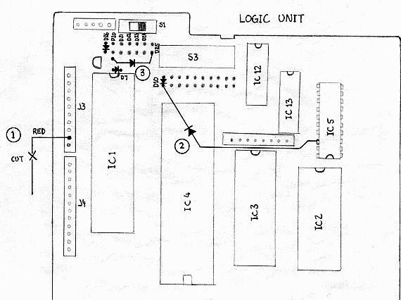
Logic Unit

MODIFICATION:
Refer to diagram above.

This modification is done to the LOGIC UNIT in three parts;

  1. Cut the red wire to J3

  2. Add a diode (small signal type ie; 1N914 etc.) between PIN 18 of IC5 74HC244 [ANODE END OF DIODE] and the CATHODE of D10 [CATHODE END OF DIODE]. The back-up battery may have to be carefully levered out of the way in order to gain better access to PIN 18 of IC5.

  3. Add a diode (small signal type ie; 1N914 etc.) between the pad where D25 CATHODE would go [CATHODE END OF DIODE] and the pad just opposite D20 CATHODE [ANODE END OF DIODE]. See diagram for details. (that's coming later)